Minimization of error is the primary purpose of PCB producers that present the critical and not critical industries. An in-depth approach to avoid the common errors, their basic roots, and protecting the heart of PCB design is the key. Because of the increasing density of these problems, there is a possibility of PCB failure. If treatment is not taken, the operations of the design will hamper the whole circuit. Eventually, it will lead to the drowning of the same. Equipment failure, burning components, and damaged traces are just a few common problems encountered by engineers while working with PCB. This asks engineers to consider frequent causes of these failures in PCB – and vital steps for problem solving and repairs.
Why does PCB fail?
PCB is successfully designed by engineers and manufactured (design of the circuit board that has been made of PCB, and fully assembled), which reliably meets its performance for its life cycle is always expected and can undoubtedly be achieved. But most of the work goes in vain because of the failure methods and layering faults. Let’s have a look at some of the general mistakes in PCB Assembly and cover the steps to mend them, in the next segment.
General PCB Failure Reasons
Layers are not in harmony
Alignment of PCB stack-up is carried out during fabrication. Assembling the board in order is a must. For instance, let’s talk of the visual approach (AOI). If it is not detected, open, shorts, or crossed signal lines can occur, which will harm board operations.
Solder Bridge
The soldering bridge is an unwanted connection among the tiny particles that constitute the Board. This may be between adjacent bearings, traces, and bearings or traces nearby. However, this can cause shorts and components or board damage.
Unfurled diagnosis
We can easily predict the future of a board by diagnosing its extended gaping. In many cases, the circuit tends to be unbarred. The PCB can, in such a case, lead to failure. Depending on the functions of the Board and the more extensive system, this might be a big disaster. For example, if the Board provides a critical measurement and this one overall system might not be managed.
Shuffled elements
If the alignment of elements in a board is not intact, it can cause damage immediately to the component or Board itself. If the current level is relatively high, the fire can break on the Board. In addition, such issues can be monitored by moisture, solder bridges that are not detected, damage to the creepage distance for high voltage boards, or unexpected events such as nails at this time.
Needs of PCB monitoring
PCB temperature issues can quickly spread to other PCB components and cause cascade damage.
Let’s have a look at some of the common forms of damage:
- Loss of the coalition integrity: Excessive heat can damage the integrity of PCB. The PCB layer is susceptible to temperature fluctuations, and when they are too hot or cold, they develop and contract. In addition, excessive heat can cause warping in length, width, and thickness of different PCB layers.
- Circuit line disorders: Excessive heat can cause damage to circuits too. The circuit line expands and changes its shape when it’s too hot. After this happens, the course becomes vulnerable to shift in frequency, distortion, and straight losses. The 50 ohms requirement can, however, be maintained with ease.
- Incompatible material expansion level: The adverse effect mentioned above is exacerbated by the fact that different materials develop at different levels. Because it contains other materials, they develop differently in response to heat. So PCBs that are too hot can experience further damage because of various types of separation layers.
- Oxidation: The PCB oxidation derives several factors that should be managed. A layer of protection should be manifested easily for confirmation and submission. In such an unavoidable case, transparent exposure to excessive heat can create turmoil. In addition, the loss of transmission channels and higher dissipation factors often occur.
Tools to prevent PCB Assembly Failure
The tool you need to solve the circuit board problem will depend on the complexity of the design. For example, solving fundamental issues may need a multimeter device, while complicated PCBs or solid components require special kit equipment, such as logical analyzers, including various LCR meters.
Some essential tools for implementing PCB repairs include:
- Clamp
- Holders
- Barriers
- Tissue
- Solder Equipment
Tips for eradication of PCB issues
The following tips help solve problems and fix problems on PCB:
Visual inspection
Conducting a visual inspection of circuit boards can help identify some problems and defects. A reasonably general problem during the distribution process in making PCB is a ‘tombstone effect’: This is where the component on the PCB is tilted at one end (how even the tombstone is set may rock with time) and therefore does not make contact with the board.
Discrete component testing
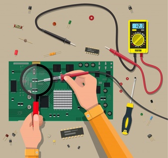
Test various PCB components, such as resistors, diodes, and capacitors, using a digital multimeter. Parts whose output value is significantly lower than specified by the manufacturer may be damaged. On the other hand, the measured value far greater than the specified value can show a problem with a soldered joint.
PCB Maintenance
If we keep a car idle for months, it fails to function efficiently. Similarly, the PCB circuit can become null if moisture and dust gather over it. Therefore, an essential step in solving problems and repairs is wiping the surface. PCB cleaning is a complicated process that requires special care and solvents to avoid damage to one of the components soldered.
As discussed, no device should be deprived of care. Be it a car or an electric circuit like PCB, proper maintenance is vital. It can otherwise lead to failure of the same. After all, while they might fail, engineers can always try to solve the issues and restore them to optimal work operations. The main difference between the approach of an engineer and a common person is the process of administration. With accuracy and integrity, the efficiency of a PCB design is restored to its full power.